Question 3
-
(a) State the purpose of biasing a transistor.
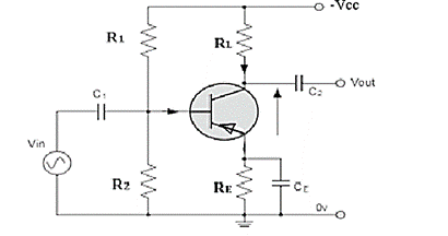
(b) Draw and label the circuit diagram of a single-stage pnp common emitter amplifier using a potential divider biasing method.
Observation
The expected responses were:
(a) Purpose of biasing a transistor
To establish the d.c. operating conditions or quiescent point (Q-point) for the desired amplification purpose.
(b)

![]() Question 3 required candidates to state the purpose of biasing a transistor and draw the circuit diagram of a single-stage pnp common emitter amplifier using a potential divider biasing method. The Chief Examiner reported that the candidates who responded to this question could not give the correct symbol of pnp transistor as well as the correct polarity for VCC for the corresponding amplifier configuration.
Question 3 required candidates to state the purpose of biasing a transistor and draw the circuit diagram of a single-stage pnp common emitter amplifier using a potential divider biasing method. The Chief Examiner reported that the candidates who responded to this question could not give the correct symbol of pnp transistor as well as the correct polarity for VCC for the corresponding amplifier configuration.
