The expected answers were:
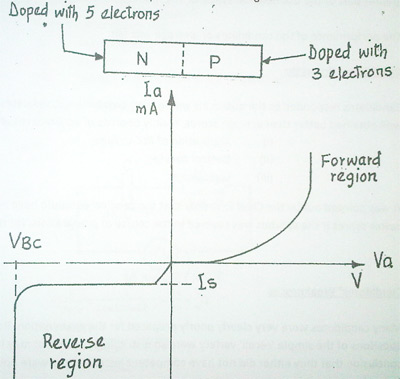
A pn junction is formed when one side of the intrinsic material is doped to form a P-
region and the other side doped to form an N-region.
(c) Application of pn junction
(i) Switch
(ii) Rectifier
(iii) Voltage stabilization
The question was on Bipolar Transistor and other Semiconductor Devices. It was quite
popular with the candidates. However, the performance was average.