
Question 1
AIM: To investigate the effect of varying load on the output of a Zener diode.
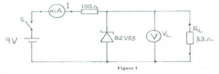
- Connect the circuit diagram as shown in Figure 1.
- Ask the Supervisor to check the circuit connection.
- Copy Table 1 into your answer booklet.
Table 1
RL(Ω) |
VL(V) |
I(mA) |
33 Ω |
|
|
47 Ω |
|
|
100 Ω |
|
|
1kΩ |
|
|
10kΩ |
|
|
- Set the power supply unit to 9V.
- Close switch (s)
- Read and record in Table 1, the ammeter and voltmeter readings.
- Open switch (s).
- Repeat steps (e) to (g) by replacing the 33Ω resistor with the other values of resistors in Table 1.
- Plot a graph of VL (V)on the vertical axis against I(mA) on the horizontal axis
- Comment on the graph.
Observation
The expected answers were:
(c) Table 1
RL(Ω) |
VL(V) |
I (mA) |
33Ω |
2.2 |
67.7 |
47 Ω |
2.9 |
61.2 |
100 Ω |
4.5 |
45.0 |
1 k Ω |
6.2 |
27.9 |
10 k Ω |
6.2 |
27.8 |
(i) A graph of VL (V) on against I (mA)
- Labeling of axes
- Line of best fit
(j) Comment on the graph
The load voltage is inversely proportional to input current
The candidates were expected to connect the circuit and take readings correctly using the appropriate measuring instruments. However, graphs plotted by a few candidates showed that they did a wrong connection of the circuit. Comments/deductions from readings were not properly stated by majority of the candidates.